Introduction
 Still complicated? Let’s get more into it
Note
All the code and resource files in this post are available on my GitHub page, because it’s fun to share.
Welcome to another part in this series. The first part is Commodore 128 assembly - Part 1.
We need to get the basics down of the Commodore 128, and so it is time to crack on with memory management. It is very important for the C128 machine code programmer to understand how this works, and it is more complicated as opposed to the C64, where memory address $01 controlled the ROM/RAM mapping in a relative simple way.
When programming the C128, the following two books are indispensable:
Also before we continue, a definition of terms:
- RAM block: a single block of 64K RAM. The C128 contains two of these;
- Bank: a configuration (combination) of RAM block selection and ROM chip mapping;
- Common RAM: an area in RAM block 0 that is also available in RAM block 1;
- MMU: Memory Management Unit, the “new $01”;
- VDC: Video Display Chip, the new video chip in the C128;
- VIC II: Video Interface Chip, the video chip as known from the C64;
- VIC Bank: an area of 16K of RAM, used by the VIC chip.
Memory Management
Take a look at this memory map, and then lets go through this one area at a time.
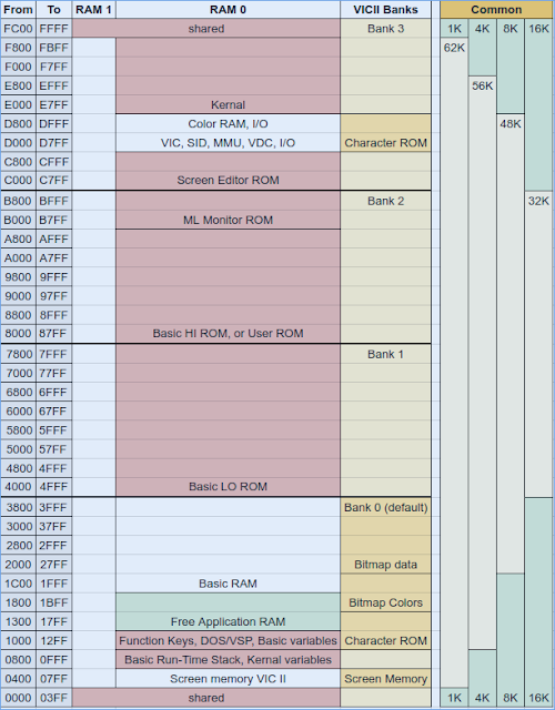 The infamous Commodore 128 memory map
When we look at the RAM0 and VICII Banks columns, we can see the C128 is much the same as the C64. There is a bigger BASIC ROM though, and some areas we know from the C64 have been moved (start of BASIC RAM, location of BASIC variables, screen editor). When we introduce the RAM1 column and the Common areas it starts to become more complicated as there are more combinations to be taken care off.
The bottom of RAM1 is used by BASIC to store variables. The rest is free to use as needed.
MMU
The chip that does all this trickery for us is the memory management unit (MMU). Its registers are mapped to $D500 to $D506. This is not inside the default common RAM block, so this introduces the problem that any configuration that maps out the ROM in this area will also make the MMU unavailable.
Commodore solved this by mirroring the MMU registers in the top of memory ($FF00) and force this area common. You should not use locations from $FF00 to $FFFF for code or data. We will use $FF00 and not $D500 for MMU configuration changes.
We will use the MMU in the following examples.
Banking
Banking is about two things:
- selecting a RAM block;
- determining which ROMS are available, or not
Being an 8 bit processor, the 8502 can only ‘see’ 64K at a time so there needs to be a mechanism to switch between the RAM blocks. This is done by selecting a bank configuration.
ROM chips can be enabled or disabled. When disabling a ROM, the RAM underneath becomes available for reading. You can always write to a RAM location ‘underneath’ a ROM.
The BASIC BANK command will select one of 15 configurations that Commodore has prepared. Bank configuration 15 is the default setting, and it provides the configuration shown in the map above.
In machine code, we need to access the MMU directly, and set the bits of the configuration register ($FF00) that we want. A macro helps with that:
.macro SetBankConfiguration(id) {
	.if(id==0) {
lda #111111  // no roms, RAM0
}
	.if(id==1) {
lda #%01111111  // no roms, RAM1
}
	.if(id==12) {
lda #000110  // int.function ROM, Kernal and IO, RAM0
}
	.if(id==14) {
lda #000001  // all roms, char ROM, RAM0
}
	.if(id==15) {
lda #000000  // all roms, RAM0. default setting.
}
	.if(id==99) {
lda #001110  // IO, kernal, RAM0. 48K RAM.
}
	sta MMUCR
}
It generates this code when we call SetBankConfiguration(15):
LDA #$00
STA $FF00
This will select RAM bank configuration 15 and enable I/O, Kernal and BASIC ROMs. The macro offers the possibility to add custom configurations (see option 99). There is also a configuration (12) that enables the internal function ROM (a free socket on the motherboard can be fitted with a custom ROM chip).
In general, try to use RAM block 0 for program code, and RAM block 1 for data.
Common RAM area
By default, common RAM is only present at the bottom of the memory map, has a size of 1K, and runs from $0000 to $03FF. Common RAM always comes from RAM block 0. The configuration of common RAM has nothing to do with banking; choosing another bank configuration does not change the common RAM settings.
If you only need to access RAM block 0, then a good place for programs is in the range of $1300 to $1BFF. If you do not use BASIC then you can use up to $3FFF. But, any program located here making the switch to RAM block 1 cannot continue as this range is outside the common area and therefore unavailable in RAM block 1. The program will crash.
When writing programs that need to use both RAM blocks, you need to put that program (or the part that accesses both blocks) in the common area. This situation was foreseen and Commodore has provided some free space in this area and subroutines for reading and writing data to and from any RAM configuration.
We will take a look at those subroutines in another part.
If your program or data is too large to fit in the default common area, then its size can be changed. It can be 1, 4, 8 or 16K in size. The macro I created to change the size is this:
.macro SetCommonRAM(amount) {
	lda MMURCR
	and #%11111100  // clear bits 0 and 1. this is also option 1
.if(amount==4) {
	ora #000001
}
.if(amount==8) {
	ora #000010
}
.if(amount==16) {
	ora #000011
}
	sta MMURCR
}
Calling SetCommonRAM(8) generates:
LDA $FF06
AND #$FC
ORA #$02
STA $FF06
Also, we can choose to make the top of memory common, the bottom (default) or both. In total we can have 32K of common RAM. This is done by using the following macro:
.macro SetCommonEnabled(option) {
	lda MMURCR
	and #%11110011  // clear bits 2 and 3
	ora #option*4
	sta MMURCR
}
Calling SetCommonEnabled(1) generates:
LDA $FF06
AND #$F3
ORA #$04
STA $FF06
This will make the bottom 8K common only.
VIC II
The VIC chip in the C128 is configured exactly the same as on the C64. The VIC chip registers are mapped onto $D000 in RAM. By default, the VIC chip uses the same 16K area as the C64 ($0000 to $3FFF) and the screen and character memory offsets are also identical.
Also, as on the C64, the VIC chip does not see ROM, only RAM. No matter what your memory configuration is, you can use the RAM you selected even if a ROM image is mapped in the same location.
As you can see in the memory map above, the VIC can be pointed to 4 blocks of RAM, also called banks… The following macro accepts a number from 0 to 3:
.macro SetVICBank (bank) {
	lda $dd00
	and #%11111100
	ora #3-bank
	sta $dd00
}
Calling SetVICBank(0) creates:
 LDA $DD00
 AND #$FC
 ORA #$03
 STA $DD00
Which will select VIC bank 0, which is the default. Are you tired of the word bank yet?
Within this 16K block of RAM, we can change the offsets to the character set data and the screen display matrix (screen memory) inside that block.
.macro SetCharacterOffset (offset) {
	lda $d018
	and #%11110001  // clear the 3 offset control bits
	ora #offset
	sta $d018
}
Calling SetCharacterOffset(4) assembles to:
 LDA $D018
 AND #$F1
 ORA #$04
 STA $D018
This mean that the offset for the character data is 4K. If the VIC bank is located at $0000 (the default) then the character data is read from $1000. As you can see from the map above, this is the default.
The offset voor screen memory (screen matrix) can be changed in 1K steps. The macro I created for this is:
.macro SetMatrixOffset (offset) {
	lda $d018
	and #001111  // clear the 4 offset control bits
	.if(offset > 0) {
		ora #offset*16
	}
	sta $d018
}
Using SetMatrixOffset(1) assembles to:
 LDA $D018
 AND #$0F
 ORA #$10
 STA $D018
Which will place the screen RAM at $0000 + $400 = $0400, which is, again, the default.
So far, nothing different from the C64. There is one new option though: you can tell the MMU that the VIC chip should use RAM block 1. Here’s the macro to do that, and it accepts a 0 or a 1 as value:
.macro SetVICRAMBank(value) {
	lda MMURCR
	and #%10111111  // clear bit 6
	.if(value==1) {
		ora #%01111111  // enable bit 6
}
	sta MMURCR
}
All Kernal routines etc work with RAM block 0, so why you would want to do this, I do not know. I accept all tips regarding this subject!
VDC
The VDC registers are absent, its registers cannot be found in the C128 memory map, except for these two: $D600 and $D601. The VDC Video RAM and registers are isolated, and are accessed via these two locations. Nothing you can do with the MMU will change the way you interact with the VDC.
Programming it is kind of a hassle, so this is where macros and some handy subroutines should make this more easy. We’ll get back to this later on.
Concluding
When planning a program for the C128, it’s wise to think about the memory layout beforehand and select or create the Bank configuration that best suits the program. It’s a good idea to draw a map like provided above, and fill in where the program and data will do. You can use the provided document I’ve shared (see the link at the top of this article)
If the VIC configuration needs changing because of the fixed location of data, then selecting another 16K block or tuning the location of character data and screen data will help.
This can now easily be done using a few macros that will generate the necessary code. Getting this out of the way will make it easier to understand the machine and plan for new programs.
Next up is Commodore 128 assembly - Part 3.